
The IISER Bhopal semiconductor cost reduction breakthrough marks a significant milestone in India’s journey toward self-reliance in advanced chip manufacturing. Researchers at Indian Institute of Science Education and Research Bhopal have developed an innovative approach that could drastically lower the cost of semiconductor fabrication — a move that aligns perfectly with India’s ambitions to boost domestic chip production amid shifting global supply chains.
As geopolitical tensions, supply disruptions, and rising manufacturing costs reshape the semiconductor industry, this IISER Bhopal semiconductor cost reduction research may provide India with a competitive edge in the global chip race..
This article explores the science, strategy, impact, and future promise of this breakthrough — providing you with a comprehensive narrative that can stand on its own or be adapted for newsletters, academic summaries, or media features. Supported by context on India’s broader semiconductor ambitions, this deep-dive aims to explain what was done, why it matters, and how it could reshape India’s technological future.
1. Why Semiconductor Chips Matter
At the heart of every modern electronic device — from smartphones and laptops to electric vehicles (EVs), medical equipment, and defence systems — lies one indispensable component: the semiconductor chip. These chips are essentially tiny electronic circuits etched into materials such as silicon that process information and power our digital world.https://ism.gov.in
Over the last two decades, semiconductors have become the backbone of the global economy, with supply chains concentrated in a few regions — notably Taiwan, South Korea, Japan, and the United States. The pandemic and geopolitical shifts exposed vulnerabilities in these supply chains, prompting many countries, including India, to pursue self-reliance in chip manufacturing.
2. The IISER Bhopal Breakthrough: What We Know
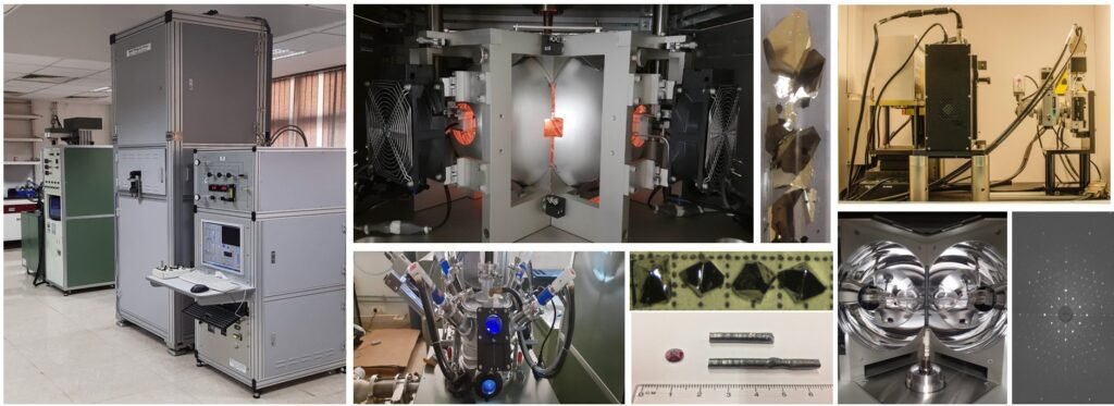
In February 2026, a team of scientists at IISER Bhopal developed a new technology that could drastically cut the cost of making modern semiconductor chips. While detailed technical specifications have yet to be publicly disclosed, media reports describe the innovation as a cost-effective method that supports low-cost chip production, potentially enabling greater affordability and accessibility in India’s chip ecosystem.
What the Innovation Could Mean
- Reduced Manufacturing Expenses: By introducing new processes or materials, the IISER team’s method promises to lower the otherwise high costs associated with semiconductor fabrication.
- Accessibility for Startups and Academia: Lower barriers could enable research labs, startups, and educational institutions to prototype and test chips without prohibitive expense.
- Boost for India’s Domestic Chip Ecosystem: This aligns directly with national goals to reduce dependency on imports and build indigenous capabilities.
Although the exact mechanism (e.g., whether it involves new lithographic techniques, alternative wafer materials, or shared fabrication strategies) is still emerging, it represents a rare academic achievement with potential industrial significance.
3. Global and National Context: India’s Semiconductor Push
India has been actively strengthening its semiconductor ecosystem through policies and programmes designed to nurture design, fabrication, and research:
Design Linked Incentive (DLI) Scheme
The Government of India’s Design Linked Incentive Scheme promotes domestic semiconductor design by offering financial incentives and infrastructure support to startups, MSMEs, and design houses. This scheme is part of a broader effort to build robust chip design capabilities within the country.
Chips to Start-up (C2S) Programme
This initiative fosters hands-on chip design experience for students and startups. It has already resulted in dozens of student-designed circuits and patents, highlighting India’s growing talent base.
Semiconductor Manufacturing Plants
In recent years, major semiconductor manufacturing facilities have been approved across multiple states, backed by billions in investment — part of the India Semiconductor Mission to strengthen manufacturing capacity.
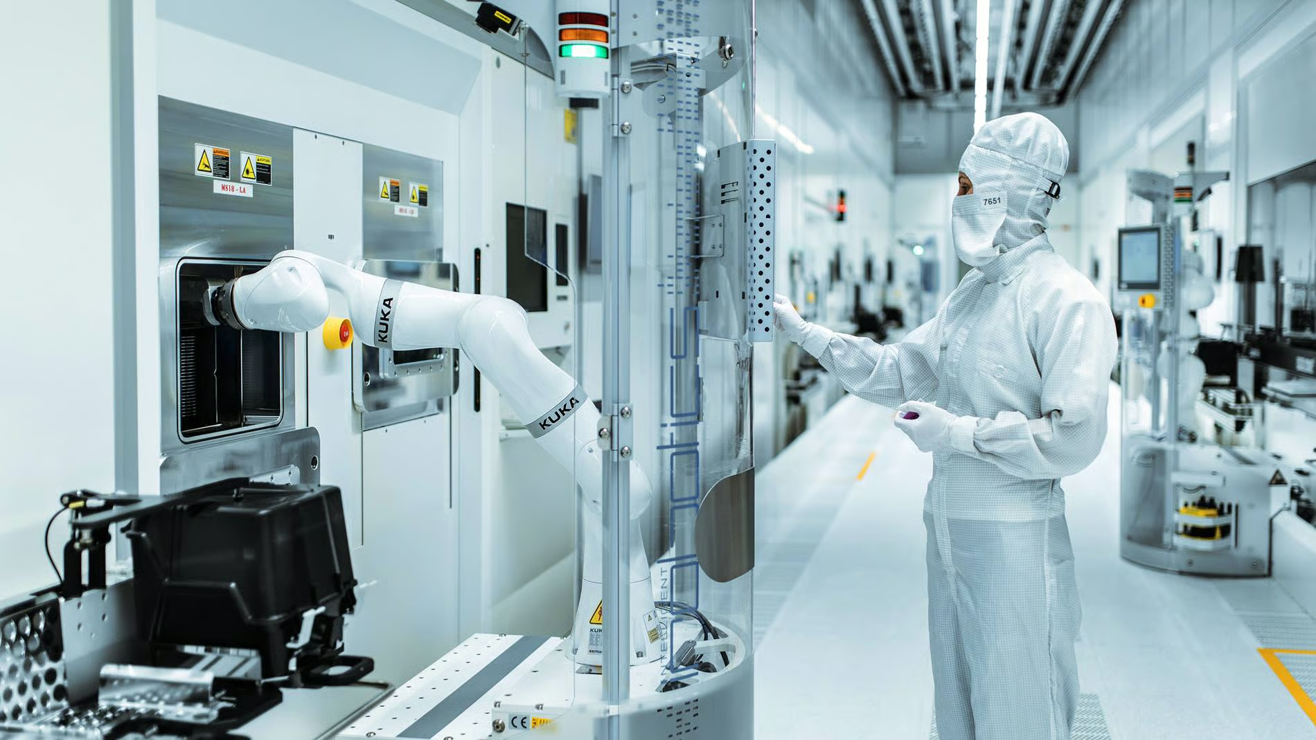
4. How Chip Manufacturing Works (Simplified)
To appreciate the significance of IISER Bhopal’s work, it’s useful to understand the basic steps in semiconductor fabrication:https://chips-dli.gov.in
From Design to Silicon
- Chip Design: Engineers create a blueprint of the circuit logic using specialized design software.
- Taping Out: Design files are converted into masks that guide chip patterning.
- Wafer Fabrication: The design is imprinted onto silicon wafers through a series of photolithography, deposition, etching, and doping processes.
- Testing and Packaging: Finished chips are tested for performance and then packaged for use.
Each of these stages is capital-intensive — especially wafer fabrication, where mask costs and cleanroom facilities are expensive.
Cost-Reducing Techniques
Modern cost-saving methods include Multi-Project Wafer (MPW) services, where multiple designs share a single wafer to split costs — reducing prototype expenses by up to 80–95%.
The IISER Bhopal method, while still under review, may employ similar strategic efficiencies or novel process innovations to achieve cost-cutting at scale.
5. What This Means for Research and Innovation
Academic institutions often struggle to access expensive semiconductor fabrication — held by large industry players. By lowering cost barriers:
- More research labs can prototype advanced chips
- Startups can innovate without massive capital investment
- A pipeline of trained talent can grow faster
This aligns with India’s goals to transform from being primarily a design hub to a full-stack semiconductor ecosystem — encompassing design, fabrication, testing, and packaging.
6. Strategic Impact on Industry and Economy
Reduced Imports, Increased Self-Reliance
India currently imports a large share of semiconductor chips — especially advanced nodes used in consumer electronics and computing. Innovations that reduce production costs help decrease this dependency over time.
Startup and SME Growth
Lower costs can fuel a new generation of homegrown semiconductor startups, enabling them to compete globally.
Jobs and Skills Development
India’s semiconductor push also emphasises workforce development — from chip design expertise to cleanroom operations — offering high-paying, future-ready jobs.
7. Challenges and What’s Next
While the innovation is promising, several challenges remain:
- Scaling from Lab to Fab: Academic breakthroughs must be translated into industrial processes.
- Infrastructure Needs: Semiconductor fabrication requires ultra-clean environments and precision equipment.
- Patent and IP Commercialisation: Protecting and commercialising the innovation will be key for industry adoption.
Research teams often collaborate with government bodies and industry partners to overcome these hurdles — and it’s likely that IISER Bhopal will continue engaging stakeholders to bring this innovation closer to production reality.
A Milestone in India’s Chip Story
The breakthrough from IISER Bhopal marks more than just a research achievement — it represents a strategic inflection point in India’s threading journey into semiconductor manufacturing. By addressing the cost and accessibility hurdles that often hinder chip innovation, this development could:/india-semiconductor-mission-explained
- Accelerate domestic chip production
- Empower startups and researchers
- Support national technology sovereignty
- And contribute to long-term economic growth
As the world continues to compete for semiconductor leadership, India’s homegrown innovations — such as this one — showcase the potential of its research ecosystem to contribute meaningfully to the global semiconductor landscape.

